Semiconductor Electronics: Materials, Devices, and Simple Circuits
Classification of solids on the basis of their conductivity(Semiconductor Electronics): On the basis of the relative values of electrical conductivity (σ) and resistivity (ρ = 1/σ), the solids are broadly classified as,
Metals: Those solids which have high conductivity and very low resistivity. The value of conductivity for metals lies in between 102 to 108 S m–1 and of resistivity between 10–2 to 10–8 W m.
Insulators: Those solids which have low conductivity and high resistivity. The value of conductivity for insulators lies between 10–11 to 10–19 S m–1 and of resistivity between 1011 to 1019 W m.
Semiconductors: Those solids which have conductivity and resistivity intermediate to metals and insulators. The value of conductivity for semiconductors lies in between 105 to 10–6 S m–1 and of resistivity between 10–5 to 106 W m.
Energy bands of solids or band theory of solids
Valence band: This band contains valence electrons. This band may be partially or completely filled with electrons. This band is never empty. Electrons in this band do not contribute to electric current.
Conduction band: In this band, electrons are rarely present. This band is either empty or partially filled. Electrons in the conduction band are known as free electrons. These electrons contribute to the electric current.
Forbidden energy gap or forbidden band: The energy gap between the valence band and conduction band is known as the forbidden energy gap or forbidden band. No electrons are present in this gap. It is a measure of energy bandgap.
– The minimum energy required for shifting electrons from valence band to conduction band is known as the energy bandgap.
– If l is the wavelength of radiation used in shifting the electron from valence band to conduction band, then the energy band gap is

Where h is called Planck’s constant and c is the speed of light.
– The forbidden energy gap Eg in a semiconductor depends upon temperature.
– Fermi energy: It is the maximum possible energy possessed by free electrons of a material at absolute zero temperature (i.e. 0 K)
Differences between metals, insulators, and semiconductors on the basis of band theory
Metals
– In metals either the conduction band is partially filled or conduction band and valence band partially overlap each other.
– In metals, there is no forbidden energy gap between the valence and conduction bands.
Insulators
– In insulators, the valence band is completely filled and the conduction band is completely empty.
– In insulators, there is a very wide forbidden energy gap between the valence and conduction bands. It is of the order of 5 eV or more.
Semiconductors
– In semiconductors, the valence band is completely filled and the conduction band is empty.
– In semiconductors, there is a small forbidden energy gap between the valence and the conduction bands. It is of the order of 1 eV.
For silicon, it is 1.1 eV and for germanium, it is 0.72 eV.
– At absolute zero, semiconductors behave as a perfect insulator.
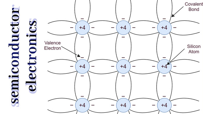
– Hole: It is a seat of positive charge which is produced when an electron breaks away from a covalent bond in a semiconductor. Hole has a positive charge equal to that of electron. The mobility of hole is smaller than that of electron.
Intrinsic semiconductor: A pure semiconductor which is free from every impurity is known as intrinsic semiconductor. Germanium (Ge) and silicon (Si) are the important examples of intrinsic semiconductors.
In intrinsic semiconductor, ne = nh = ni where ne , nh are number density of electrons in conduction band and number density of holes in valence band, ni is the intrinsic carrier concentration.
When an electric field is applied across an intrinsic semiconductor, electrons and holes move in opposite directions so that total current (I) through the pure semiconductor is given by
I = Ie + Ih
Where Ie is the free electron current and Ih is the hole current.
Effect of temperature on the conductivity of intrinsic semiconductor
– An intrinsic semiconductor will behave as a perfect insulator at absolute zero.
– With increasing temperature, the density of hole-electron pairs increases and hence the conductivity of an intrinsic semiconductor increases with an increase in temperature.
In other words, the resistivity (inverse of conductivity) decreases as the temperature increases.
– The semiconductors have negative temperature coefficient of resistance.
Doping: It is a process of deliberate addition of a desirable impurity to a pure semiconductor in order to increase its conductivity. The impurity atoms added are known as dopants.
Extrinsic semiconductor: A doped semiconductor is known as extrinsic semiconductor. Extrinsic semiconductors are of two types:
N-type semiconductor
– When a pure semiconductor of Si or Ge (tetravalent) is doped with a group V pentavalent impurities like arsenic (As), antimony (Sb), phosphorus (P) etc, we obtain an n-type semiconductor. The pentavalent impurity atoms are known as donor atoms.
– It is called n-type semiconductor because the conduction of electricity in such semiconductor is due to motion of electrons i.e. negative charges.
– It is called donor type semiconductor, because the doped impurity atom donates one free electron to semiconductor for conduction.
– In n-type semiconductor electrons are majority carriers and holes are minority carriers.
– The representation of n-type semiconductor is as shown in the figure.

– n-type semiconductor is neutral.
– In n-type semiconductor ne ≈ Nd > > nh where Nd is the density of donor atoms.
p-type semiconductor
When a pure semiconductor of Si or Ge (tetravalent) is doped with a group III trivalent impurities like aluminium (Al), boron (B), indium (In) etc, we obtain a p-type semiconductor. The trivalent impurity atoms are known as acceptor atoms.
– It is called p-type because the conduction of electricity in such semiconductor is due to motion of holes i.e. positive charges.
– It is called acceptor type semiconductor because the doped impurity atom creates a hole in semiconductor which accepts the electron, resulting conduction in p-type semiconductor.
– In p-type semiconductor, holes are majority carriers and electrons are minority carriers.
– The representation of p-type semiconductor is as shown in the figure.

– p-type semiconductor is neutral.
– In p-type semiconductor nh ≈ Na > > ne
Where Na is the density of acceptor atoms.
Mass action law: Under thermal equilibrium, the product of the free negative and positive concentrations is a constant independent of the amount of donor and acceptor impurity doping. This relationship is known as the mass action law and is given by
Where ne , nh are the number density of electrons and holes respectively and ni is the intrinsic carriers concentration.
p–n junction: When donor impurities are introduced into one side and acceptors into the other side of a single crystal of an intrinsic semiconductor, a p-n junction is formed. It is also known as junction diode. The most important characteristic of a p-n junction is its ability to conduct current in one direction only. In the other (reverse) direction it offers very high resistance. It is symbolically represented by

Depletion region: In the vicinity of the junction, the region containing the uncompensated acceptor and donor ions is known as the depletion region. There is a depletion of mobile charges (holes and free electrons) in this region. Since this region has immobile (fixed) ions that are electrically charged it is also known as the space charge region.
The electric field between the acceptor and the donor ions is known as a barrier. The physical distance from one side of the barrier to the other is known as the width of the barrier. The difference of potential from one side of the barrier to the other side is known as the height of the barrier.
– For a silicon p-n junction, the barrier potential is about 0.7 V, whereas for a germanium p-n junction it is approximately 0.3 V.
– The width of the depletion layer and magnitude of potential barrier depend upon the nature of the material of semiconductor and the concentration of impurity atoms. The thickness of the depletion region is of the order of one tenth of a micrometre.
Forward biasing of a p–n junction: When the positive terminal of external battery is connected to p-side and negative to n-side of p-n junction, then the p-n junction is said to be forward biased.
– In forward biasing, the width of the depletion region decreases and barrier height reduces.
– The resistance of the p-n junction becomes low in forward biasing.
Reverse biasing of a p–n junction: When the positive terminal of the external battery is connected to n-side and the negative terminal to p-side of a p-n junction, then the p-n junction is said to be reverse biased.
– In reverse biasing, the width of the depletion region increases and barrier height increases.
– The resistance of the p-n junction becomes high in reverse biasing.
Breakdown voltage: A very small current flows through p-n junction, when it is reverse biased. The flow of the current is due to the movement of minority charge carriers. The reverse current is almost independent of the applied voltage. However, if the reverse bias voltage is continuously increased, for a certain reverse voltage, the current through the p-n junction will increase abruptly. This reverse bias voltage is thus known as breakdown voltage. There can be two different causes for the break down. One is known as Zener breakdown and the other is known as avalanche breakdown.
Ideal diode: A diode permits only unidirectional conduction. It conducts well in the forward direction and poorly in the reverse direction. It would have been ideal if a diode acts as a perfect conductor (with zero voltage across it) when it is forward biased, and as a perfect insulator (with no current flows through it) when it is reverse biased.
An ideal diode acts like an automatic switch.
In forward bias, it acts as a closed switch whereas in reverse bias it acts as an open switch as shown in the figure:-

Rectifier: It is a device which converts ac voltage to dc voltage. Diode is used as a rectifier. Rectifier is based on the fact that, a forward bias p-n junction conducts and a reverse bias p-n junction does not conduct.
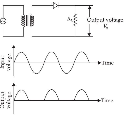
Half wave rectifier: Diode conducts corresponding to the positive half cycle and does not conduct during the negative half cycle. Hence, AC is converted by diode into unidirectional pulsating DC. This action is known as halfwave rectification.
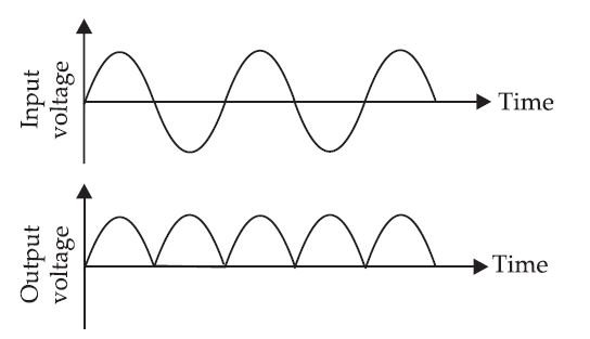
Full-wave rectifier: The circuit diagram, input and output waveforms for a full wave rectifier are as shown in the figure.

Ripple factor: The ripple factor is a measure of the purity of the dc output of a rectifier, and is defined as

Special Purpose p–n Junction Diodes
light-emitting diode (LED): It converts electrical energy into light energy. It is a heavily doped p-n junction which operates under forwarding bias and emits spontaneous radiation.
– The I-V characteristics of a LED is similar to that of Si junction diode. But the threshold voltages are much higher and slightly different for each colour. The reverse breakdown voltages of LEDs are very low, typically around 5 V.
– The semiconductor used for the fabrication of visible LEDs must at least have a band gap of 1.8 eV. The compound semiconductor gallium arsenide phosphide (GaAsP) is used for making LEDs of different colours. GaAs is used for making infrared LED.
– The symbol of a LED is shown in the figure.

Photodiode: A photodiode is a special type p-n junction diode fabricated with a transparent window to allow light to fall on the diode. It is operated under reverse bias. When it is illuminated with light of photon energy greater than the energy gap of the semiconductor, electron-hole pairs are generated in near depletion region.
– The symbol of a photodiode is shown in the figure below.

Solar cell: It converts solar energy into electrical energy. A solar cell is basically a p-n junction that generates emf when solar radiation falls on the p-n junction. It works on the same principle (photovoltaic effect) as the photodiode, except that no external bias is applied and the junction area is kept large.
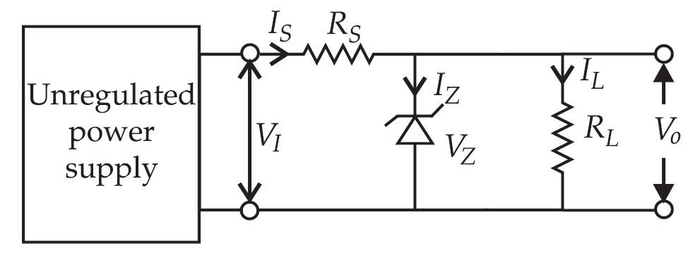
Zener diode: It was invented by C. Zener. It is designed to operate under reverse bias in the breakdown region and is used as a voltage regulator. The symbol for Zener diode is shown in the figure.

– Zener diode as a voltage regulator: The circuit diagram for Zener diode as a voltage regulator is shown in the figure below.
Transistor
A junction transistor is a three-terminal semiconductor device consisting of p–n junctions formed by placing a thin layer of doped semiconductor (p. type or n-type) between two similar layers of the opposite type. There are two types of transistor :
(i) p–n–p transistor: Here, two segments of n-type semiconductor (emitter and collector) are separated by a segment of p-type semiconductor (base).
(ii) p–n–p transistor: Here two segments of p-type (termed as emitter and collector) are separated by a segment of n-type semiconductor (base).
The schematic representations of a n-p-n and p-n-p transistors are shown in the figure.
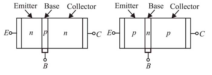
The symbols for n-p-n and p-n-p transistors are shown in the figure below.

In operation of a transistor, IE = IB + IC
Where IE emitter is current, IB is base current, IC is the collector current.
A transistor can be operated in any one of the following three configurations:
- – Common emitter (CE)
- – Common base (CB)
- – Common collector (CC)
Input characteristics of a transistor
The variation of the input current with the input voltage for a given output voltage is known as the input characteristics of a transistor.
Output characteristics of a transistor
The variation of the output current with the output voltage for a given input current is known as output characteristics of a transistor.
Common emitter amplifier: In the common emitter transistor amplifier, the input signal voltage and the output collector voltage are 180° out of phase.
Transistor as an oscillator: An oscillator generates AC output signal without any input ac signal. An oscillator is a self-sustained amplifier in which a part of the output is fed back to the input in the same phase (this process is called positive feedback).
Logic Gates
A digital circuit with one or more input signals but only one output signal is known as a logic gate. There are three basic logic gates:
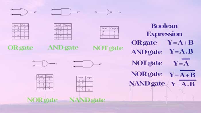
OR gate: An OR gate has two or more inputs but only one output.
– The logic symbol of OR gate is
– The truth table for OR gate is
– The Boolean expression for OR gate is Y = A + B
AND gate: An AND gate has two or more inputs but only one output.
– The logic symbol of AND gate is
– The truth table for AND gate is
– The Boolean expression for AND gate is Y = A·B
NOT gate: The NOT gate is the simplest of all logic gates. It has only one input and one output.
– The logic symbol of NOT gate is
– The truth table for NOT gate is
– The Boolean expression for NOT gate is Y = A
NAND gate: It is an AND gate followed by a NOT gate.
– The logic symbol for NAND gate is
– The truth table for NAND gate is
– The Boolean expression for NAND gate is Y = A⋅ B
NOR gate: It is an OR gate followed by a NOT gate.
– The logic symbol of NOR gate is
– The truth table for NOR gate is
– The Boolean expression for NOR gate is Y = A + B
