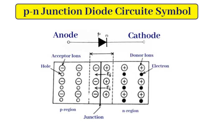
The direction of the arrow, which is from p to n, represents the direction of effect of conventional current in the forward biasing junction. The p side is called the anode and the n side is called the cathode.
How p-n Junction Diode works : Forward and Reverse Biasing
p-n junction diode is a basic semiconductor device. It is a semiconductor crystal which has an excess of acceptor impurities in one region and donor impurities in the other region.
These regions are called p-region and n-region respectively and the boundary between these regions is called p-n junction diode.
The positive holes in the p-type region are the majority charge carriers and have the same number of stable negative acceptor ions.
Similarly, in the n-region, negative electrons are the majority charge carriers and there are equally stable positive donor ions. Thus both the regions are electrically neutral.
Formation of Depletion layer : Potential barrier :
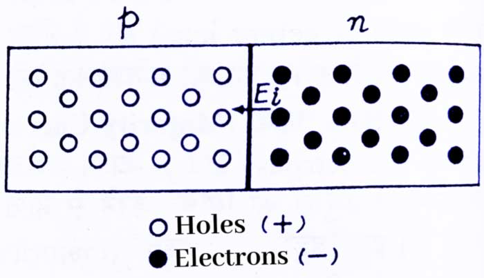
As soon as p-n junction is formed, due to thermal disturbance, diffusion of majority of charge carriers across the junction starts.
Some electrons from the n-region diffuse into the p-region, and some holes from the p-region diffuse into the n-region.
After diffusion, these charge-carriers become neutral together with their counterparts. Thus, near the junction, positive charge (in the form of stable donor ions) in the n-region and negative charge (in the form of stable acceptor ions) in the p-region gets accumulated.
This creates a potential difference across the junction and establishes an internal valid region Ei which is directed from the (plus) n-region to the (minus) p-region. After some time the valid region becomes so strong that further diffusion of majority of charge carriers stops.

The layer on either side of the junction in which there are no mobile charge carriers is called ‘depletion layer’. The thickness of the depletion layer is of the order of 10-6 meters. The potential difference between its ends is called the potential barrier.
Its value is about 0.3 volts for germanium p-n junction, and about 0.7 volts for silicon p-n junction. The potential wall depends on the concentration of the impurity mixed in the semiconductor and on the temperature of the junction.
Flow of current in p-n junction diode :
If there is no external battery in a junction diode, then no current is carried in it. Some of the majority carriers (holes in the p-region and electrons in the n-region) have so much energy that they cross the junction against the region Ei of the potential wall and take the form of current.
But this current is precisely canceled out by the reverse current produced by minority carriers (electron in p-region and hole in n-region). So that the net current is zero in junction diode.
Junction diodes can be connected to an external battery in two different ways, which are called forward biasing and reverse biasing.
Forward Biasing :
When the p-region of the junction diode is connected to the positive end of the external battery, and the n-region to the negative end, then the junction is said to be forward biased.
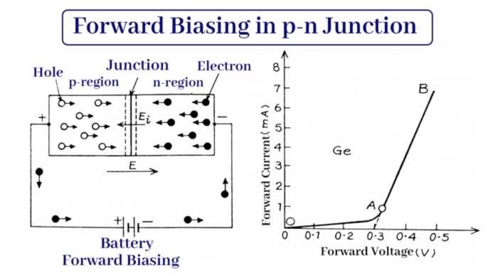
In this case an external valid region E is established in the diode which is directed from p-region to n-region. region E, the internal validity is much stronger than-region Ei. Therefore, the hole in the p-region and the electron in the n-region both move towards the junction.
- Importance of Biomolecules in Life || What are the 4 main biomolecules?
- Resonance effect or mesomeric effect || What is resonance effect with example?
- Valency of Elements || How to Find Valency || What is the Valency of the atom?
- Glucose Structure: Physical and chemical properties, Glucose Chemical Reaction
- Introduction of Inductive-Effect || How does Inductive Effect Work?
(The holes move in the direction of region E and in the opposite direction of electron E.) They get extinct after reaching near the hole and electron junction and combine with each other. For each electron-hole combination, a covalent bond is broken in the p-region near the positive end of the battery.
The hole generated by this moves towards the junction while the electron enters the positive end of the battery through the connecting wire.
At the same time, an electron is released from the negative end of the battery and enters the n-region and takes the place of the electron lost by coincidence near the junction.
Thus, the movement of the majority carriers establishes a valid current in the junction diode. This is called forward current.
In a forward biasing junction, since the applied electric field E is stronger than the internal field Ei, the majority carriers (holes in the p-region and electrons in the n-region) are pulled towards the junction. This reduces the width of the depletion-region.
This is the reason that the forward biasing junction diode has a low resistance to current flow.
The difference between the forward voltage applied at the junction and the forward current received is shown in the graph. Initially, the current in the junction diode is almost zero due to the opposing potential ramp.
- How p-n Junction Diode works : Forward and Reverse Biasing
- Semiconductors : How Semiconductor works and Types
- X-Rays – Production, Properties, Wavelength and Uses
- Daily use Chemical Compounds and Their Properties
- Hard Water and Soft Water : Permutit and Anion Exchange Resins
On increasing the applied voltage, the current increases very slowly and non-linearly. until the voltage exceeds the potential ramp. This behavior of the diode is represented by the part OA of the voltage current curve.
On increasing the applied voltage further, the current increases rapidly and almost linearly. At this point the diode behaves like a normal conductor.
This behavior is represented by the straight line AB of the curve. If the placed AB is extended backwards, then it cuts the voltage axis at the potential gate voltage.
Reverse Biasing :
When the p-region of the junction diode is connected to the negative end of the external battery, and the n-region to the positive end, then the junction is said to be reverse biased.
In this case the external valid region E is directed from the n-region to the p-region, and thus it supports the internal ramp-region Ei.
Now both the hole in the p-region and the electron in the n-region start moving away from the junction. Hence they can never coincide near the junction. It is clear that no current flows through a diode because of the majority of carriers.
But when there is junction reverse biasing, a very small reverse current flows across the junction. It is generated from thermally generated minority carriers that cross the junction within the legitimate region E.
Since the number of minority carriers depends on the thermal disturbance, the reverse current depends heavily on the temperature and increases as the temperature of the junction increases.
- Importance of Biomolecules in Life || What are the 4 main biomolecules?
- Resonance effect or mesomeric effect || What is resonance effect with example?
- Valency of Elements || How to Find Valency || What is the Valency of the atom?
- Glucose Structure: Physical and chemical properties, Glucose Chemical Reaction
- Introduction of Inductive-Effect || How does Inductive Effect Work?
In reverse biasing junction, the applied electric field E reinforces the internal field Ei, so the majority carriers tend to move away from the junction. This increases the width of the depletion-region.
This is the reason why reverse biasing junction diode has a very high resistance to current flow.
The difference between the reverse voltage applied at the junction and the received reverse current is shown in the graph. Since the internal boundary region Ei also helps in the movement of minority carriers, all the carriers cross the junction.
Due to this the reverse current is almost constant over a very large range of applied reverse voltage. This behavior of the diode is represented by the OC part of the voltage current curve.
Avalanche Breakdown :
When the reverse biasing voltage becomes too high, the minority carriers acquire a lot of kinetic energy so that the covalent bonds near the junction are broken and the electron-hole pairs are freed.
These charge carriers also accelerate and release other electron hole pairs in the same way. This process is cumulative and a large number of electron-hole pairs are liberated. Then the value of reverse current suddenly increases a lot.
This situation is called Avalanche breakdown.
And there is a possibility of damage to the junction due to the heat generated due to the current. The reverse voltage at which the reverse current increases suddenly is called breakdown voltage. Its numerical value depends on the density of the impurity atoms in the diode.
Avalanche Breakdown :
In electronic circuits, semiconductor devices are represented by symbols. The symbol of p-n junction diode is shown below. In this, arrow – head denotes p-region and bar denotes n-region.
