How Transistor Works : PNP and NPN Transistors
Transistors
It is such an electronic device made of p and n-type semi conductor which is used in place of triode bulb.
It was invented in 1948 by American scientists John Bardeen, William B. Shockley and Walter H. Brattain. For this they were awarded the noble prize in 1956.
There are two types of transistors:
p-n-p transistor
n-p-n transistor
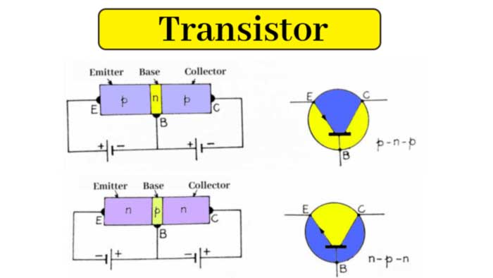
p-n-p Transistor
In this, a very fine slice of n-type semiconductor is inserted between two small pieces of p-type semiconductor.
The middle slice is called the base (B), the left side is called the emitter (E) and the right side is called the collector (C). The emitter is given a positive potential with respect to the base and the collector is given a negative potential.
Thus, the emitter base (p-n) junction on the left is forward biased with low resistance and the base collector (n-p) junction on the right is reverse biased, with high resistance.
The symbol of pnp transistor is shown below. In this, the direction of the arrow shows the direction of the current.

n-p-n Transistor
In this a very fine slice of p type semiconductor is inserted between two small blocks of n type semiconductor.
In this transistor, negative potential is given to the emitter, relative to the base, and positive potential to the collector. Again the emitter base (n-p) junction on the left is forward biased and the base collector (p-n) junction on the right is reverse biased.
The symbon of npn transistor is given below.

In this, the direction of the arrow shows the direction of the current. The emitter provides the majority carrier for the current to flow. And the collector collects these carriers. The base controls the movement of charge carriers from the emitter to the collector.
Transistor Circuits
Transistor can be connected in any circuit in three ways. Their names:
Common – base configuration
Common – emitter Configuration
Common – collector Configuration
How p-n-p transistor works
The common base circuit of p-n-p transistor is shown in the image below. The emitter base (p-n) junction on the left is given a low forward biased potential by an emitter base battery Veb, while the base collector (n-p) junction on the right is given a large reverse biased potential by another battery Vcb.

Being forward biased, the holes present in the emitter, move towards the base, while the electrons present in the base move towards the emitter.
Since the base is very thin, most of the entering holes (near about 98%) pass through it to the collector, while very few of them combine with the electrons present in the base.
A new electron reaches the positive end of the battery (Veb) as soon as it combines with a hole electron. This creates a hole in the emitter which starts moving towards the base. Thus a weak current flows in the base emitter circuit.
Those who enter the hole collector, which is reverse biased and helps the holes to operate, reach terminal C. As soon as one reaches hole C, an electron from the negative end of the battery Vcb neutralizes it.
At this very moment a covalent bond breaks in the emitter. The electron generated from this comes out of the emitter through terminal E and enters the positive end of the battery web and starts moving towards the hole. Thus, valid current flows through the collector emitter circuit.
It is clear that the current flow inside the p-n-p transistor is due to the holes moving from the emitter to the collector. Whereas it is due to the movement of electrons in the external circuit.
- How Transistor Works : PNP and NPN Transistors
- How p-n Junction Diode works : Forward and Reverse Biasing
- Semiconductors : How Semiconductor works and Types
- X-Rays – Production, Properties, Wavelength and Uses
- Daily use Chemical Compounds and Their Properties
- Hard Water and Soft Water : Permutit and Anion Exchange Resins
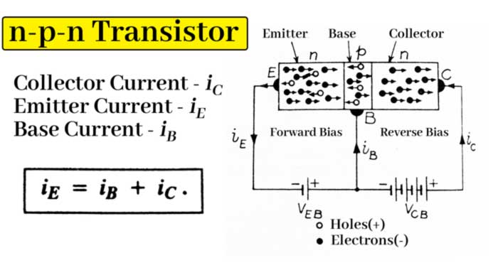
The current flowing from terminal B is called base current ib and the current going out of terminal C of collector is called collector current ic. These two currents together enter the emitter terminal E, which is called emitter current iE.
Because the base is very thin, the number of hole-electrons that can be combined into it is very small. In this way almost all the holes that enter the base from the emitter reach the collector. Therefore the collector current iC is only slightly less than the emitter current iE.
How n-p-n transistor works
The common base circuit of the n-p-n transistor is shown in the image below. Both the n regions have mobile electrons while the thin p region in the middle has mobile holes.
The emitter base (n-p) junction on the left is given a slight forward biased potential by the battery Veb, while the base collector (p-n) junction on the right is given a large reverse biased potential by the battery Vcb.
Being forward biased, electrons move from emitter (n-region) towards base, while holes move from base (p-region) towards emitter. Since the base is very thin, most of the electrons entering it cross it and reach the collector.
Only a few combine with the holes present in the electron base. As soon as an electron combines with a hole, in the same way an electron exits from the negative end of the battery web and enters the emitter through terminal E.
At this very moment, a Covalent bond breaks in the base, the electron generated by it enters the positive end of the battery web and the hole compensates for the hole lost due to coincidence. Thus current flows in the base emitter circuit.
- Importance of Biomolecules in Life || What are the 4 main biomolecules?
- Resonance effect or mesomeric effect || What is resonance effect with example?
- Valency of Elements || How to Find Valency || What is the Valency of the atom?
- Glucose Structure: Physical and chemical properties, Glucose Chemical Reaction
- Introduction of Inductive-Effect || How does Inductive Effect Work?
- IUPAC Name : How to find the IUPAC name of compounds.
Those who enter the electron collector, which is reverse biased and helps the electron to move, reach terminal C. As soon as an electron leaves the C and enters the positive end of the battery Vcb, similarly an electron from the negative end of the battery Veb enters the emitter. Thus current flows in the collector emitter circuit.
It is clear from the above that there are electron charge carriers inside the npn transistor and also in the external circuit.
The small current entering the terminal B of the base is the base current iB and the large current entering the collector terminal C is the collector current iC. These two currents together come out from the emitter terminal E which is the emitter current iE.
Comparison of p-n-p and n-p-n transistors:
Although the working system of both types of transistors is same, but the charge carrier in p-n-p transistor is mainly hole whereas in n-p-n transistor the charge carrier is mainly electron.
Electrons are more dynamic than holes. Therefore, only n-p-n transistors are used in high frequency circuits and computers where the response to the signals of the carriers must be very quick.